PCB Design Best Practices for IoT Products

PCB Design Best Practices for IoT Products
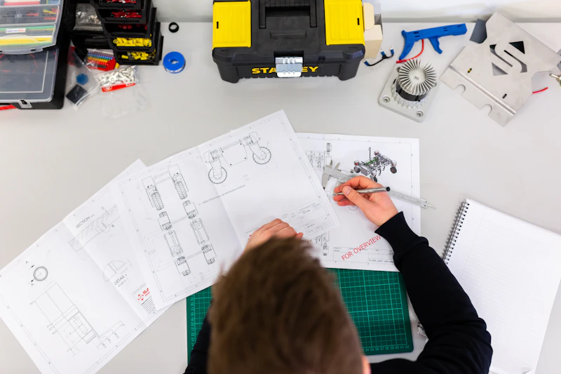
Designing a PCB for an IoT product isn't the same as hobbyist prototyping. When your board goes into production, every trace width, via placement, and component footprint matters. Here are the practices we follow at Its Your Turn.
1. Start with the Right Stack-Up
For most IoT products, a 4-layer stack-up is the sweet spot:
| Layer | Purpose | |-------|---------| | Top | Signal + Components | | Inner 1 | Ground Plane | | Inner 2 | Power Plane | | Bottom | Signal + Components |
A solid ground plane is essential for:
- Reducing EMI emissions
- Providing clean return paths
- Improving signal integrity for high-speed traces
2. Antenna Placement Rules
IoT boards almost always have an antenna — WiFi, BLE, LoRa, or Zigbee. Follow these rules:
- Keep the antenna area clear — No copper pour, no traces, no components in the antenna keep-out zone
- Place at board edge — Maximize radiation efficiency
- Match impedance — 50Ω trace from RF pin to antenna
- Add a ground plane cutout — As specified by the antenna manufacturer
3. Power Supply Design
A clean power supply is the foundation of reliable IoT hardware.
[Battery/USB] → [LDO/Buck] → [3.3V Rail] → [MCU + Sensors]
                                           → [RF Module]
Key considerations:
- Use bulk capacitors (100µF) at the regulator output
- Place decoupling capacitors (100nF) as close to IC power pins as possible
- Separate analog and digital ground planes, join at a single point
- Add ferrite beads on the RF power supply
4. Design for Manufacturing (DFM)
Your design must be manufacturable at scale:
- Minimum trace width: 6 mil (for standard fab houses)
- Minimum via size: 0.3mm drill, 0.6mm pad
- Component spacing: 0.2mm minimum between pads
- Fiducial markers: At least 3 for pick-and-place alignment
- Panelization: Design break-away tabs for automated assembly
5. Testing & Validation
Before sending to production:
- DRC (Design Rule Check) — Run this in Altium/KiCad to catch violations
- ERC (Electrical Rule Check) — Verify all nets are connected correctly
- Thermal Analysis — Ensure power components have adequate copper pour for heat dissipation
- Prototype First — Always order 5-10 PCBs from JLCPCB or PCBWay before committing to production runs
6. Documentation Package
A complete handoff to manufacturing includes:
- Gerber files (RS-274X format)
- Drill files (Excellon format)
- Bill of Materials (BOM) with manufacturer part numbers
- Assembly drawings (top and bottom)
- Pick-and-place centroid file
- Schematic PDF for reference
Common Mistakes to Avoid
- ❌ Routing high-speed signals near board edges
- ❌ Using thin traces for power delivery
- ❌ Ignoring thermal relief on ground pads
- ❌ Not adding test points for debugging
- ❌ Forgetting to add silkscreen labels for connectors
Want to master PCB design? Explore our Hardware Design & PCB track.